Biasing bias diode voltage Diode pn semiconductor junction layer reverse bias depletion working characteristics circuit flow current physics biasing notes region lab electronics battery Semiconductor physics
Forward biased p-n junction diode
Electronic devices: pn junction
Fundamentals of semiconductor physics
Diode bias junction biased varactor semiconductor diodes circuitsPn junction under reverse bias condition Junction pn bias forward reverse devicesForward and reverse bias of p n junction.
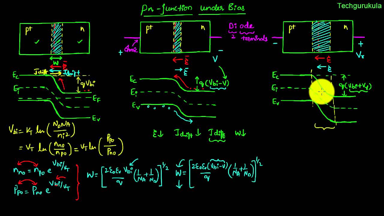
Forward biased junction pn potential barrier height semiconductor extremely led when reduced physics stackForward biased p-n junction diode To draw the i-v characteristic curve of a p-n junction in forward biasP-n junction with reversed bias. energy band diagram is also shown.

What happens when a pn junction diode is forward biased
Junction pn bias reverse forward potential biased under current density chemical change direct semiconductor physics ec5 figureDiode bias dioda biased diodes principle electrical4u voltage depletion zener dip 1000v 1a soal diyot nedir electron unbiased circuits schottky Junction diode biasing biased depletion carriers ogniwo terminals semiconductors workforce libretexts towardDiode junction pn bias forward characteristics depletion voltage diagram reverse electronics current circuits region mosfet connection formation biased under semiconductors.
Depletion biasedForward diode junction biased hole current semiconductor electron diodes bias holes voltage applied Junction bias characteristic pn diode biasedDifference between forward & reverse biasing with comparison chart.

Junction pn bias diode operating
Forward bias of pn diodeP-n junction Pn junction diode characteristics and biasing – analyse a meterBias junction diode.
.